 1
1Declare each length scale
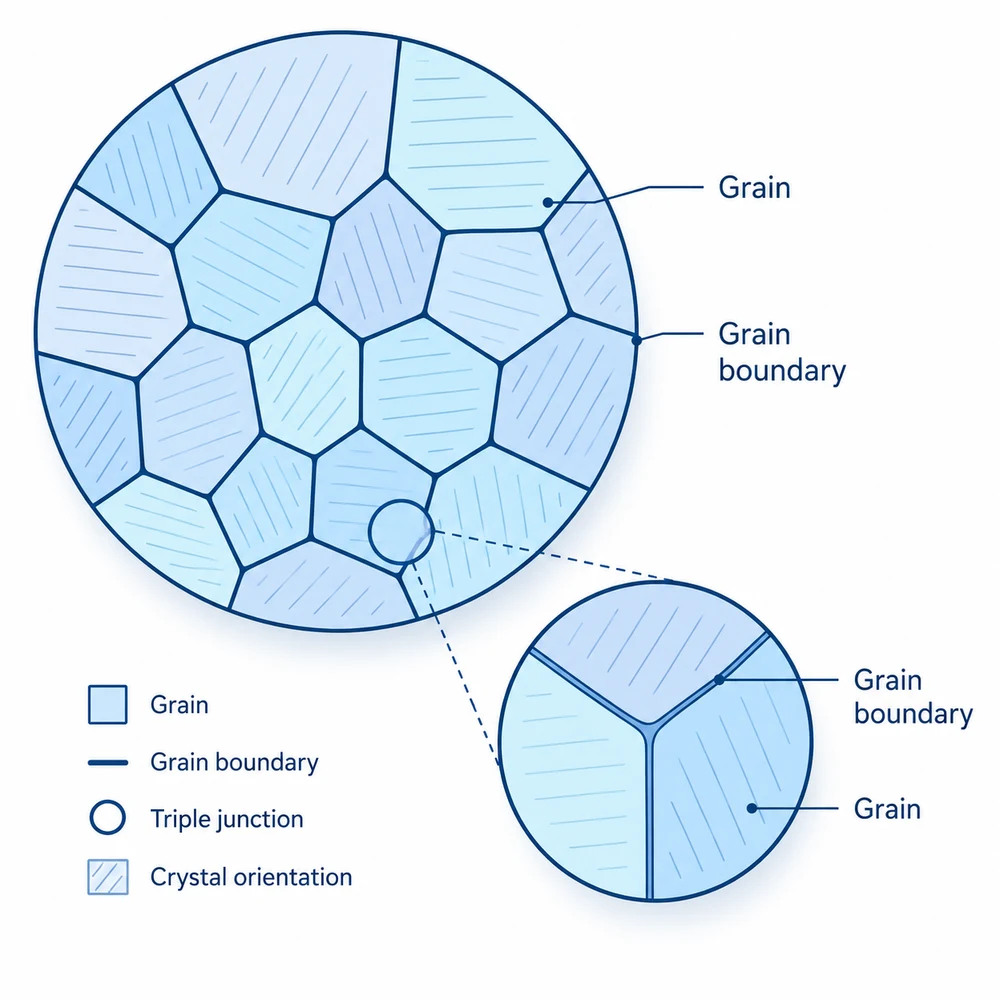
Separate atomic lattice, nanoscale feature, grain, film, component, and complete device. Use inset boundaries and scale labels so readers do not interpret a conceptual transition as a continuous physical view.
- Name composition, phase, orientation, and interface
- Mark schematic views as not to scale
- Use source microscopy for observed morphology
- Keep crystal axes and device axes distinct